

Digital Communications: A Discrete-Time Approach
by Michael Rice

A Complete QPSK System
Introduction
The previous QPSK Simulink exercises assumed perfect synchronization, perfect timing synchronization, or perfect phase synchronization. It is now time to explore how it is in practice--neither carrier phase nor timing is known to the detector and must be estimated. Simultaneous carrier phase and symbol timing synchronization is an example of a joint estimator: more than one unknown parameter is estimated. This is accomplished using two PLLs, one for timing synchronization (the inner loop) and one for carrier phase synchronization (the outer loop). The issue of carrier phase ambiguity is still with us, so differential encoding is also used here.In this exercise, you will design a joint carrier phase ans symbol timing timing synchronizer for QPSK based on two PLLs. There are three sample rates in play in this design, so you must be careful in assigning sample times to the Simulink blocks. The detector, with its accompanying bit timing synchronizer, will be used to process the modulated sampled in the file qpskcompletedata.mat.
Textbook References
M-ary QAM: Section 5.3, discrete-time realizations: Section 5.3.2, partial response pulse shapes: Section A.2, discrete-time PLL: Section C.2, carrier phase synchronization for QPSK: Section 7.2, differential encoding for phase ambiguity resolution for QPSK: Section 7.7.2, general discussion of timing synchronization: Section 8.1, discrete-time techniques for symbol timing synchronization for binary PAM: Section 8.4, discrete-time techniques for symbol timing synchronization for MQAM: Section 8.5.Specifications
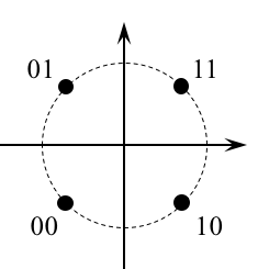 |
|

Preliminary Design
Design the Detector
Design the detector, shown below, using blocks from the Simulink, DSP System, and Communications System Toolboxes.
- Design the symbol timing loop filter to create a second order loop whose closed-loop equivalent bandwidth = 0.01 (normalized to the symbol rate) and whose damping factor is 0.7071.
- Design the carrier phase loop filter to create a second order loop whose closed-loop equivalent bandwidth = 0.02 (normalized to the symbol rate) and whose damping factor is 0.7071.
Design Notes
- Because the early-late TED operates at 2 samples/symbol, the matched filter outputs are downsampled by 4.
- The carrier phase synchronization loop is the outer loop shown in red.
- In the two previous two Simulink exercises devoted to carrier phase synchronization for QPSK (Carrier Phase Synchronization for QPSK Using the Unique Word and Carrier Phase Synchronization for QPSK Using Differential Encoding/Decoding), perfect timing synchronization was assumed and this assumption allowed the carrier phase PLL to operate at one sample per symbol.
- In contrast, the matched filter outputs here are at 2 samples/symbol. Consequently, the CCW rotation block operates at 2 samples/symbol.
- The PED operates at 2 samples/symbols, but only updates at 1 sample/symbol. This is why the PED needs to strobe input. When the strobe is asserted, the PED output follows the formula (7.26). When the strobe is not asserted, the PED output is 0. (For those of you familiar with multirate discrete-time processing, this is like an upsample-by-two operation.)
- The loop filter and DDS operate at 2 samples/symbol. (In the context of multirate processing, the PED does the upsample-by-two and the loop filter is the "interpolating filter" to smooth out the inserted zeros.)
- The symbol timing PLL is the inner loop shown in blue. Except for the CCW rotation block, the symbol timing PLL is identical to the one you designed for the Symbol Timing Synchronization for QPSK Simulink Exercise.
- Use a Farrow interpolator. You can use either the piecewise-parabolic version (Figure 8.4.17) or the cubic version (Figure 8.4.18).
- For interpolation control, use the decrementing modulo-1 counter described in Section 8.4.3. Use the underflow condition in the decrementing mod-1 counter as the strobe. The strobe is used as an enable signal for the TED, PED, decision, and mu update.
- You need to create an "enabled" version of the early-late TED. When the strobe is asserted, the TED output is given by equation (8.34). When the strobe is not asserted, the TED output is zero.
- For the fractional interval (mu) update, use an "enabled hold" block.
The "enabled hold" block outputs the previous value when the strobe is not asserted,
or passes the input to the output when the strobe is asserted.
This block is needed because the fractional interval is updated by the mod-1
counter only once per symbol, but the interpolator operates at 2 samples/symbol.
The hold operation ensures that the interpolator is using the proper value for
the fractional interval.
Simulink provides a skeletal enabled subsystem:
Simulink -> Ports & Subsystems -> Enabled Subsystem
The default enabled subsystem is shown below
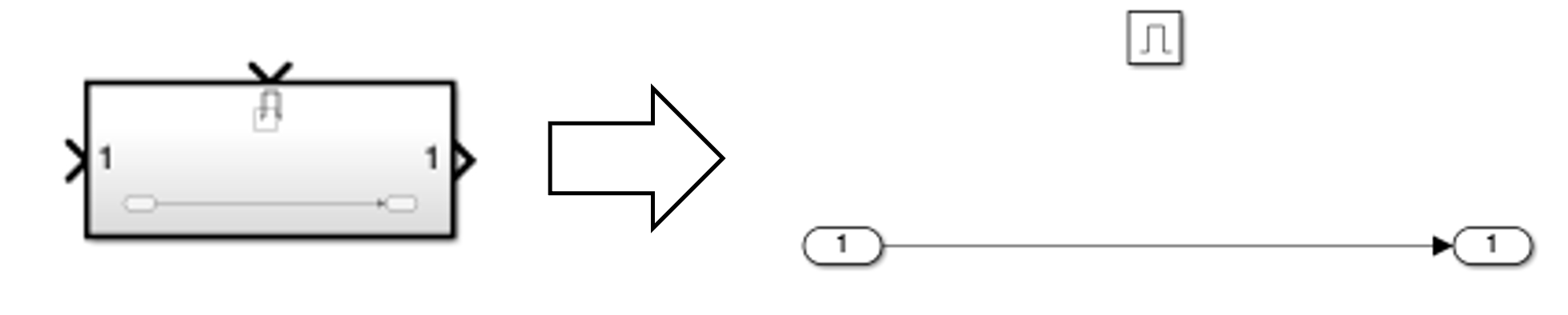
The subsystem consists of a simple wire with the enable icon above it. This means the wire is only active when the enable signal is asserted. When the enable signal is not asserted, nothing happens and the output holds its value. -
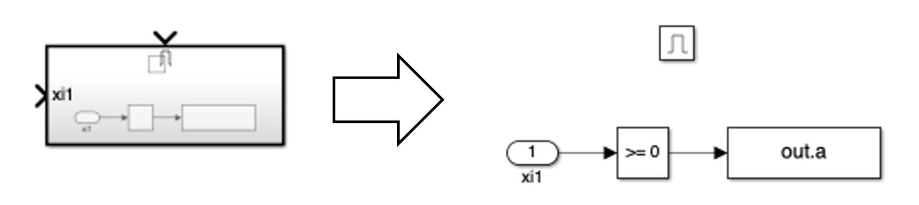
The decision subsystem is also enabled.
This is because decisions should be made on every other interpolator output on average.
The strobe indicates which interpolator outputs
represent the desired signal space projections.
An example of the enabled decision subsystem for binary PAM is shown below
Exercise
- Incorporate the carrier phase and symbol timing synchronization PLLs into a QPSK detector.
- For the detector input, use the From File block and set the Filename to qpskcompletedata.mat and the sample time to 1.
-
Set the simulation parameters as follows:
Simulation time Start Time: 0.0 Stop time:(12+500+2898+8+2)*8 Solver selection Type: Fixed-step Solver: discrete (no continuous states)
The stop time includes an additional two symbol times to account for a sample rate mismatch. The input is sampled at approximately 8 samples/symbol. - Run the simulation.
- The detector produces approximately 3420 symbol decisions. (The exact number depends on the number of times the strobe is high. This, in turn, depends on the dynamics of your symbol timing PLL.)
- To find the data, look for the 8-symbol (16 bit) SYNC pattern in the detector output. Once you find it, the following 2989 symbol decisions correspond to 828 7-bit ASCII characters. Determine the message using either your Matlab script or an ASCII Table.
- Plot the filtered phase error (loop filter output) and use this plot to estimate how long (measured in symbols) it took for your carrier phase PLL to lock.
- Plot the fractional interpolation interval (mu) and use this plot to estimate how long (measured in symbols) it took for your timing PLL to lock.
Brigham Young University - Provo |
Fulton College of Engineering |
The Church of Jesus Christ of Latter-day Saints
Department of Electrical and Computer Engineering, BYU, Provo, UT 84602 - (801)422-4012 - Copyright 2009. All Rights Reserved
Department of Electrical and Computer Engineering, BYU, Provo, UT 84602 - (801)422-4012 - Copyright 2009. All Rights Reserved